Emerging Technologies Research for Semiconductor Materials
Overview
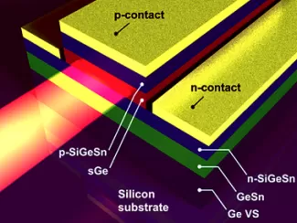
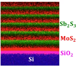
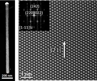
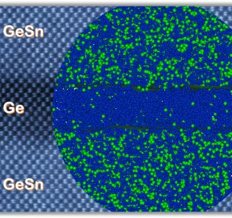
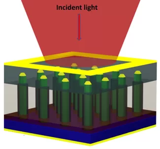
The ability to tap into nanoscale and quantum scale phenomena in semiconducting materials can create a myriad of opportunities to achieve novel, scalable, and integrable technologies with potential impact on diverse areas of science and engineering. Considering this context, we aim to combine unique nanofabrication and integration processes to develop an atomistic understanding of the science of epitaxial growth of semiconductors and implement nanoscale probes to test their properties and functionalities. The associated research programs will strive for excellence and aim for the highest impact on advanced fundamental studies as well as technological implications for the next generation of nanoelectronics, optoelectronics, photonics, clean-energy harvesting, bio-integrable, and quantum technologies.

According to NASSCOM, by 2025 AI and data science will account for about 10 per cent of India’s GDP.
AI Specialists and Data Scientists fall under the highest-growth job roles of tomorrow according to LinkedIn’s 2020 Emerging Jobs Report
Adroit Market Research states that by 2025, data science will be a USD 178 bn industry.
Research Faculty

Dr. Samik Mukherjee
Assistant Professor, Jio Institute